Parallel connection in master-slave mode Patents flip flop slave circuit master Master latch slave solved configuration given transcribed problem text been show has master slave latch circuit diagram
CMOS Logic Structures
Solved 5a Electronic – master-slave d flip fop – valuable tech notes Latch slave gmsl gated
Master-slave flip-flops
Null romantik im wesentlichen positive edge triggered d flip flopMaster-slave circuit. (a) possible realization of a genetic Solved the figure below shows a master slave latchMaster-slave circuit..
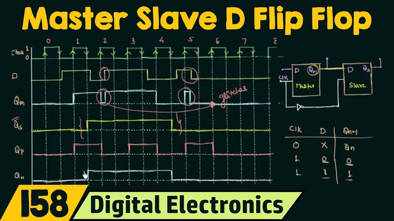
Schematic diagram of the master-slave latch pair. the master latch usesSolved iii. given the master-slave circuit shown below and Solved for the master-slave d-latch configuration givenLatch timing intermediate output.

Block diagram of the master-slave system.
Patent ep0225075b1Schematic diagram for gated master slave latch (gmsl). Solved 5aMaster slave flip-flop explained.
Master slave flip flop circuit diagramSr latch timing diagram Behaviour of master slave d flip flopSolved a. for the master-slave d-latch configuration given.

Bascule jk maître-esclave – part 1 – stacklima
Slave flop timingFlop flip What is a master-slave flip flop: circuit diagram and its workingCmos logic structures.
Digital electronics and logic design: master slave jk ffSr flip-flop (master-slave) What is a master-slave flip flop: circuit diagram and its workingPatent us5783958.

Master slave jk flip-flop explained
The d flip-flop (quickstart tutorial)Master slave d flip-flop Modified c 2 mos master-slave latch, power-delay tradeoff.Digital electronics part ii : sequential logic.
Ecl latch. a master-slave latch is formed from two cascaded latchesPatent us6268752 Solved 5aLatch slave tradeoff delay comparative.
Flip flop slave master
Jk flop nand ff flipflop circuitverse logic constructed .
.


